Wire bonding has remained a fundamental interconnection technique across the semiconductor industry and microelectronics for 70 years.
High-quality, durable connections rely entirely on the absolute cleanliness of bonding surfaces. Today, dry and scalable quattroClean snow-jet technology has emerged as a reliable, cost-effective method to achieve this precision.
The critical role of cleanliness in interconnection technology
Wire bonding spans applications from automotive systems and consumer products to MEMS, industrial sensors, battery cells, and energy storage. Stefan Schmitz, Managing Director of Bond-IQ GmbH and initiator of the Surf:Guide industry project, notes: “Wire bonding is generally divided into three major process groups. Two of these are fine-wire processes, in which - depending on the application - wires made of gold, silver, aluminum, or copper with diameters ranging from 18 to 50 µm are used. The third group involves thick-wire bonding with wire diameters ranging from 100 to 500 µm,”.
Because bonds form in the nanometre range, the targeted metals must reach an atomic state relative to one another. Consequently, residues as small as 5 to 10 µm can severely hinder operations. Problematic residues include:
Fingerprints and bleeding adhesives
Dust and flux residues
Outgassing from various polymers
Oxides and remnants from wet-chemical cleaning
“Visually detectable contamination is critical for bonding. If this contamination is no longer visible after cleaning, the bonding surface is usually sufficiently clean. This can generally be determined using a microscope and a visual before-and-after comparison. This alone can increase the success rate three- to fourfold,” explains Stefan Schmitz.
Evaluating methods for surface preparation
Historically, bonding surfaces have been prepared using wet chemical processes relying on solvents or water-based media, which necessitate energy-intensive drying phases. While plasma and laser cleaning offer alternatives for specific contaminants, they present unique limitations.
“For very sensitive surfaces, such as those in microelectronics, however, the costs of a laser system and the appropriate laser technology must first be balanced,” explains Stefan Schmitz. “The industry is currently showing interest in quattroClean snow-jet cleaning, as it can also remove more stubborn, encrusted contaminants.”
Sustainable cleaning with quattroClean
The cleanroom-compatible quattroClean snow-jet technology provides a robust dry cleaning process for full-surface or localised applications. It systematically removes particulate contaminants down to the submicrometre range and film-like residues to the nanolayer level.
This method utilises liquid, purified carbon dioxide sourced from chemical production and biomass energy generation. The medium travels through a dual-component ring nozzle, expanding into fine snow crystals. Concentrated by a compressed air jet, these crystals are propelled at supersonic speeds onto the target. As the carbon dioxide completely sublimates, surfaces remain entirely dry. Dislodged contaminants are extracted alongside the gas, preventing recontamination. This process holds the Green Screen certification for cleaners and degreasers.
Diverse applications across modern manufacturing
The exceptionally low abrasiveness of snow crystals allows the quattroClean technology to safely treat finely structured surfaces, including clearing flux from printed circuit boards (PCBs) and cleaning battery cells.
“The process can be used very efficiently on printed circuit boards, which often have a mixture of organic residues such as grease, fingerprints, flux, or residues from wet chemical cleaning processes. We have also achieved excellent results on semiconductors and on housings that have undergone electroplating or other wet chemical processes,” reports Stefan Schmitz.
The straightforward automation of this technology enhances its industrial appeal. “This results in two advantages. First, automated cleaning ensures reproducible, uniform results. Second, when cleaning is integrated into the manufacturing process, freshly deposited contaminants can be removed immediately,” Stefan Schmitz adds.
acp systems AG will showcase these advancements at Electronica in hall A2, booth 112, in Munich from 10 to 13 November 2026.
acp systems AG redefines wire bonding with CO₂ snow-jet cleaning
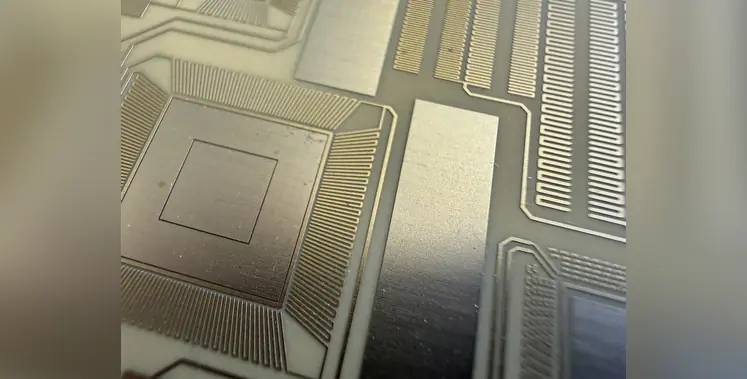
acp systems AG will showcase these advancements at Electronica in hall A2, booth 112, in Munich from 10 to 13 November 2026.